| |


Next: Transport Control Module
Up: Control Board
Previous: Fader Module
Contents
A single output assignment module is present in the prototype control
board. Figure 74 shows the silkscreen/assembly layer
for the output assignment PC board. Table 3 lists
the bill of materials for this board. Figures 75 and
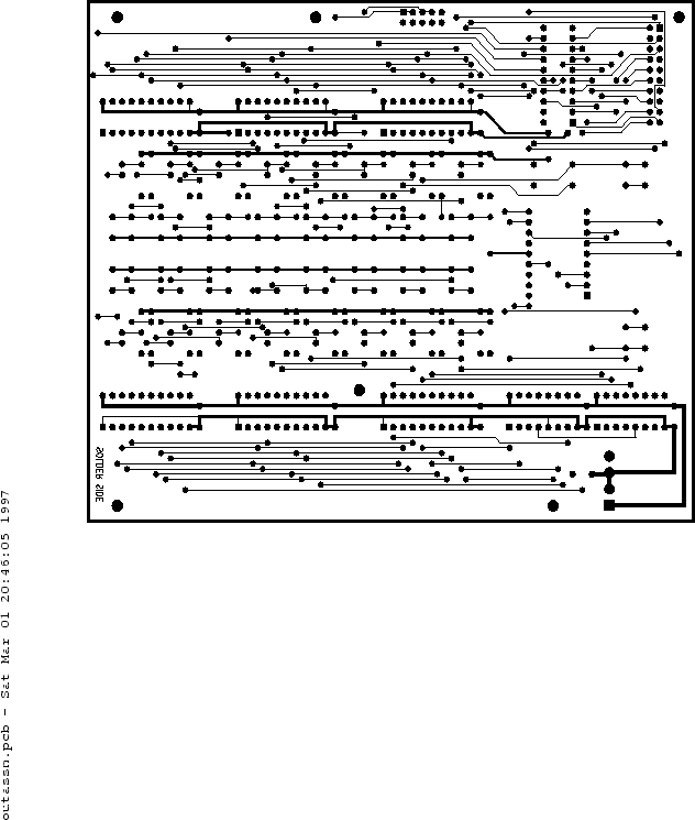
76 show the top and bottom routing layers, respectively.
Figure 74:
Output assign module PCB, silkscreen/assembly drawing.
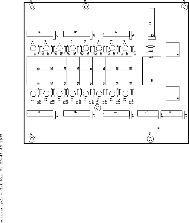 |
Table 3:
Output assign module, bill of materials.
| REFDES |
QTY |
DESCRIPTION |
| S1 - S18 |
18 |
E-Switch momentary PCB-mount pushbutton |
| R1 - R16 |
16 |
300 ohm 1/8W |
| R17 - R34 |
18 |
2.2K ohm 1/8W |
| C1 - C9 |
9 |
0.1uF monolithic |
| C10 |
1 |
10uF electrolytic |
| D1 - D16 |
16 |
T1-3/4 green LED |
| D17 |
1 |
dual 7-segment green LED display |
| U1 - U6 |
6 |
74LS373 |
| U7, U8 |
2 |
74LS247 |
| U9 |
1 |
GAL16V8 |
| J1 |
1 |
20-pin DIP header |
| J2 |
1 |
4-pin 0.156in. power connector |
| J3 |
1 |
10-pin DIP header |
|
Figure 75:
Output assign module PCB, component-side routing.
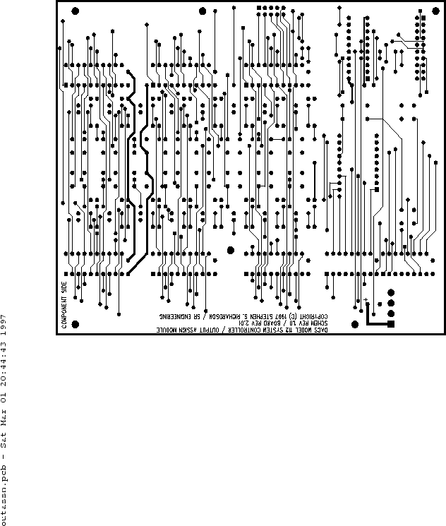 |
Figure 76:
Output assign module PCB, solder-side routing.
 |
Next: Transport Control Module
Up: Control Board
Previous: Fader Module
Contents
Steve Richardson
2000-07-06
|
Table of Contents
![[PDF]](/~prefect/images/pdficonsmall.gif) [Whole document in PDF 1.9MB]
[Whole document in PDF 1.9MB]
[more photos and information]
|